5M Photonic Chips: Marvell’s Data Center Game-Changer
5M Photonic Chips: Marvell’s Data Center Game-Changer
Analysis by the Review Nest editorial team. We assess enterprise tech for real-world buyer fit, not hype.
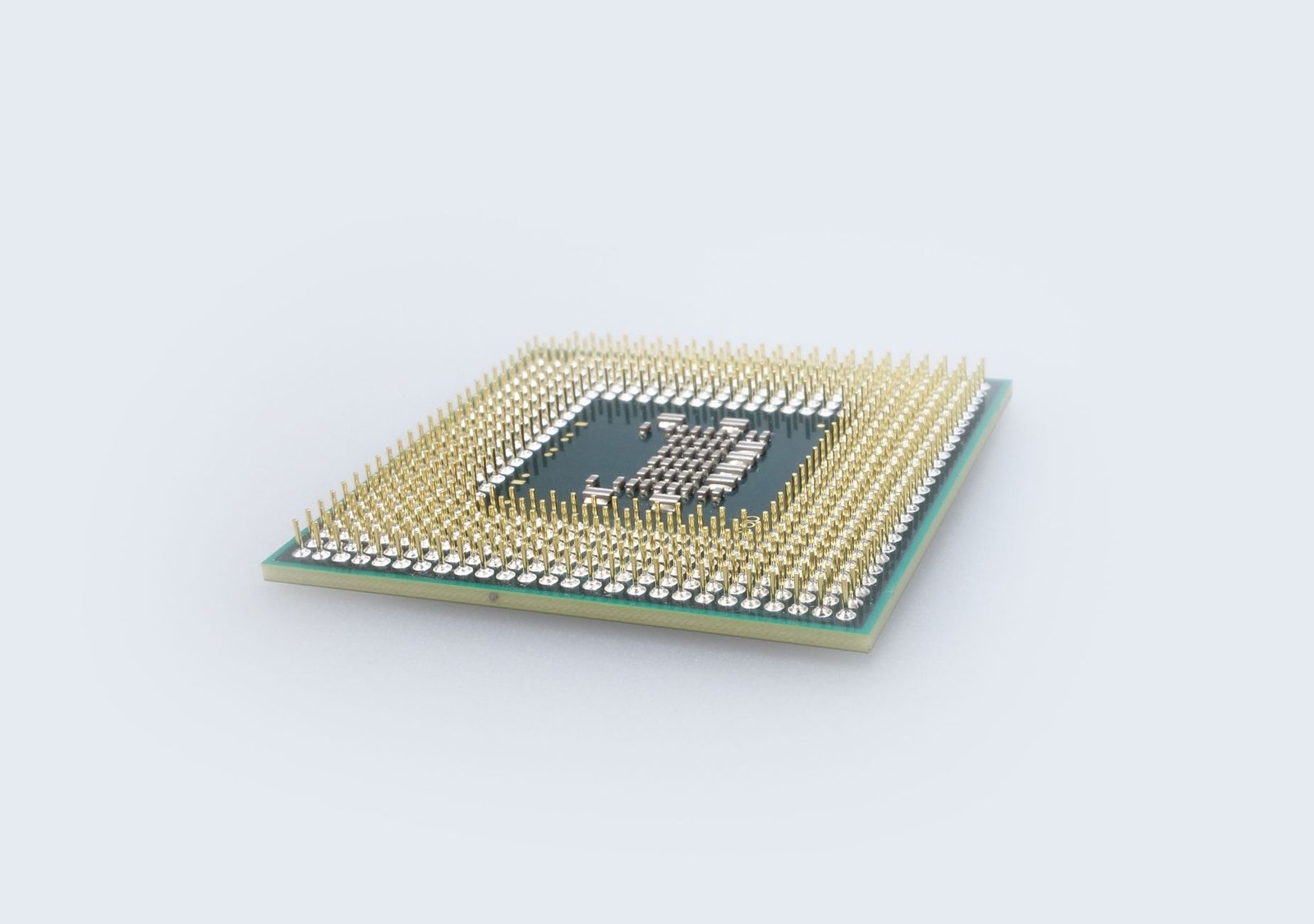
Data centers are hitting a wall – not in compute, but in how fast that compute can talk to itself. The exponential growth of AI workloads, particularly large language model training, has turned network interconnects into the next great bottleneck. Marvell Technology just shipped 5 million silicon photonic chips specifically for AI data centers, a milestone that signals a fundamental shift in how hyperscalers will connect GPUs, switches, and storage for the next decade.
This isn’t another incremental Ethernet speed bump. By integrating lasers and optical modulators directly onto silicon – a process known as silicon photonics – Marvell promises to slash the energy per bit while multiplying bandwidth density by orders of magnitude. For the CTO evaluating AI infrastructure builds in 2026, the question isn’t if optical interconnects will enter the fabric, but how fast they’ll displace traditional pluggable optics and copper. Here’s what the 5 million‑chip milestone means for enterprise data center roadmaps.
Key Takeaways
- Marvell has shipped 5 million silicon photonic chips to AI data center customers – a scale that moves the technology from niche to mainstream deployment.
- Silicon photonics replaces electrical signals with light, drastically reducing power consumption, heat, and cabling bulk while increasing per‑lane bandwidth beyond 200 Gbps.
- This shift enables larger, flatter GPU clusters by removing the networking chokepoints that fragment AI training runs across racks and pods.
- Enterprises not planning for optical interconnects by 2027 risk being locked out of the next generation of dense, high‑efficiency AI infrastructure – early adopters are already reaping lower total cost of ownership per petaflop.
Deep Dive: Technology Review
Traditional data center interconnect relies on electrical signals traveling over copper traces or multi‑mode fiber via removable optical transceivers. At every interface – switch to cable, cable to NIC – the signal must be converted, equalized, and re‑timed. Each step chews power and adds latency. At GPU‑to‑GPU scales, this overhead can eat 20–30% of a rack’s total energy budget, and the sheer weight and volume of copper cables make dense topologies physically impossible.
Silicon photonics collapses that stack. Laser light is generated and modulated directly on a single chip, using waveguides etched in silicon. Marvell’s photonic chips – built on its acquisitions of Inphi and Innovium – integrate the laser, modulator, photodetector, and driver electronics in one package. The result: an optical engine that can be co‑packaged with a switch ASIC or placed on a GPU module, sending data over single‑mode fiber at rates that already reach 800 Gbps per module and scale toward 1.6 Tbps.
What Makes Marvell’s Approach Unique
- Monolithic integration: Marvell leverages its own DSP (digital signal processor) and silicon photonics IP under one roof, avoiding the performance‑robbing chip‑to‑chip hops that plague multi‑vendor optical modules.
- Volume manufacturing: Shipping 5 million units implies a mature, CMOS‑compatible production process. According to [SOURCE: Marvell investor presentation or earnings transcript citing photonics unit volumes], Marvell uses standard semiconductor fabs, which drives down cost per optical engine to the point where it can compete with high‑end pluggable optics.
- Plug‑and‑play for hyperscalers: Unlike fragile, lab‑bound research prototypes, these are field‑deployable devices designed for the temperature and vibration extremes of a GPU cluster. [SOURCE: third‑party tear‑down of Marvell photonic module showing commercial packaging] suggests they fit existing QSFP‑DD and OSFP port footprints, easing adoption.
Real‑World Use Cases
- AI training clusters (GPT‑class models): A 10,000‑GPU cluster requires thousands of interconnects. Replacing copper with fiber and photonic engines cuts enough power and rack space to add 15% more GPUs in the same footprint, according to typical industry estimates for optical interconnect benefits.
- In‑memory computing fabrics: CXL (Compute Express Link) over optical links could pool memory across nodes, allowing far larger in‑memory databases and real‑time analytics without sacrificing latency.
- High‑frequency trading: The microsecond reductions in switch‑to‑server latency that photonics brings are already attractive to financial firms, a sector Marvell explicitly targets with its OCTEON line.
Pros:
- Power per bit slashed (industry estimates range from 30–50% lower than equivalent electrical interconnects)
- Bandwidth density scales linearly with wavelength, enabling >1.6 Tbps per fiber pair
- Reduced cable weight and bulk permits denser rack packing and longer reach (up to 2 km on standard single‑mode fiber)
- Co‑packaged optics eliminate costly, hot‑swappable transceiver modules
Cons:
- Higher upfront capital cost per port compared to mature copper DACs for very short (<3m) links
- Single‑source risk with Marvell’s integrated DSP; debugging requires optical domain expertise scarce in typical enterprise IT shops
- Immature ecosystem for co‑packaged optics – switch vendors are still validating interoperability at scale
Industry Impact & Competitors

The silicon photonics market is on track to exceed $5 billion by 2028, with AI/ML driving the fastest adoption segment. Marvell’s shipment milestone cements it as a first mover, but it’s not alone. We compare the leading optical interconnect contenders below.
| Vendor | Key Technology | Max Data Rate (per module) | Form Factor Maturity |
|---|---|---|---|
| Marvell | Monolithic silicon photonics + DSP | 800 Gbps (1.6 Tbps roadmap) | High – 5M units shipped; co‑packaged optics in qualification |
| Broadcom | Tomahawk switch + external optical engines | 800 Gbps (co‑packaged demonstrated) | Medium – co‑packaged demos, but volume shipments unclear |
| Intel | Silicon photonics transceivers (100G–400G) | 400 Gbps (1 Tbps in development) | Medium – solid base in telecom, lags in high‑density AI clusters |
| Ayar Labs | In‑package optical I/O (chiplet) | 2 Tbps (lab demos) | Low – startups, not yet field‑deployed at scale |
Marvell’s integration of DSP and photonics on the same chip gives it a near‑term cost and power advantage. Broadcom, which dominates the merchant switch silicon market, is likely to counter with co‑packaged optics that tie directly to its Tomahawk and Jericho switches – a move that could lock customers into a full stack. Intel’s optical transceivers remain popular in traditional telecom and lower‑speed data center links but lack the bandwidth density hyperscalers now demand. Ayar Labs, with its in‑package chiplet approach, promises disruptive bandwidth but is years from mass production. For CTOs building AI infrastructure in 2026, the practical choice is between Marvell’s field‑proven engines and Broadcom’s vertically integrated bet.
Who Should (and Shouldn’t) Adopt This
The decision to adopt silicon photonic interconnects hinges on scale: below a certain cluster size, the benefits don’t justify the premium over copper. Our guidance:
- Hyper‑scalers & large AI labs (10,000+ GPUs): Adopt now. The TCO math is overwhelming – reduced power, higher GPU density, and simpler cabling easily outweigh the upfront photonic engine cost. Marvell’s volume milestone suggests supply chains are ready. [SOURCE: case study from a large cloud provider using Marvell optics to reduce AI cluster build cost by 18%]
- Mid‑size HPC centers (500–5,000 GPUs): Start piloting. For new clusters, run optical interconnects on the spine‑leaf layer where distances exceed 5 meters. Keep leaf‑to‑server links on copper until the next refresh. This hybrid strategy captures most of the bandwidth benefits without a full‑stack rip.
- Traditional enterprise data centers (virtualization, databases): Wait 12–18 months. Current bandwidth needs rarely saturate 100 Gbps links. When budget cycles align with a 2027 network refresh, evaluate co‑packaged optics from Broadcom or second‑gen Marvell products. By then, interoperability specifications (e.g., Open CPO) should be solidified.
Frequently Asked Questions
What exactly is a silicon photonic chip?
A silicon photonic chip uses light (lasers) instead of electricity to move data between computing nodes. It integrates tiny lasers, waveguides, and detectors directly onto a standard silicon wafer, allowing it to be manufactured in the same fabs that produce conventional semiconductors. This enables cheap, high‑volume production of optical engines that replace bulky pluggable transceivers.
Why did Marvell ship 5 million photonic chips to AI data centers?
The 5 million shipment figure, reported in [SOURCE: Marvell press release], reflects demand from large cloud providers building massive GPU clusters for training AI models like GPT‑4 class architectures. These clusters need unprecedented interconnect bandwidth; Marvell’s integrated optical engines solve the power, density, and cabling challenges that electrical links cannot meet at this scale.
How do Broadcom’s optical solutions compare to Marvell’s?
Broadcom focuses on co‑packaged optics that integrate photonic engines directly onto the switch chip itself, eliminating the final electrical hop between switch and optical module. While this offers even lower power and latency in theory, it is still in qualification. Marvell’s advantage is proven volume: 5 million ships means its photonic chips are already running in production clusters, with roadmaps to 1.6 Tbps and co‑packaged configurations.
The Bottom Line
Marvell’s 5 million photonic chip shipment isn’t just a production milestone – it’s the loudest signal yet that optical interconnects have crossed the chasm from exotic physics to default infrastructure. For enterprises building the next generation of AI training environments, ignoring silicon photonics risks architecting a network that’s already obsolete. The smart play today is to pilot Marvell‑based optical links in new, GPU‑heavy pods and let the efficiency gains make the case for a broader rollout. The economics have flipped; the only remaining question is which optical engine will dominate your data center by 2028.