3 Reasons Intel’s Lens Partnership Is a Game-Changer for AI Chips
3 Reasons Intel’s Lens Partnership Is a Game-Changer for AI Chips
Analysis by the Review Nest editorial team. We assess enterprise tech for real-world buyer fit, not hype.
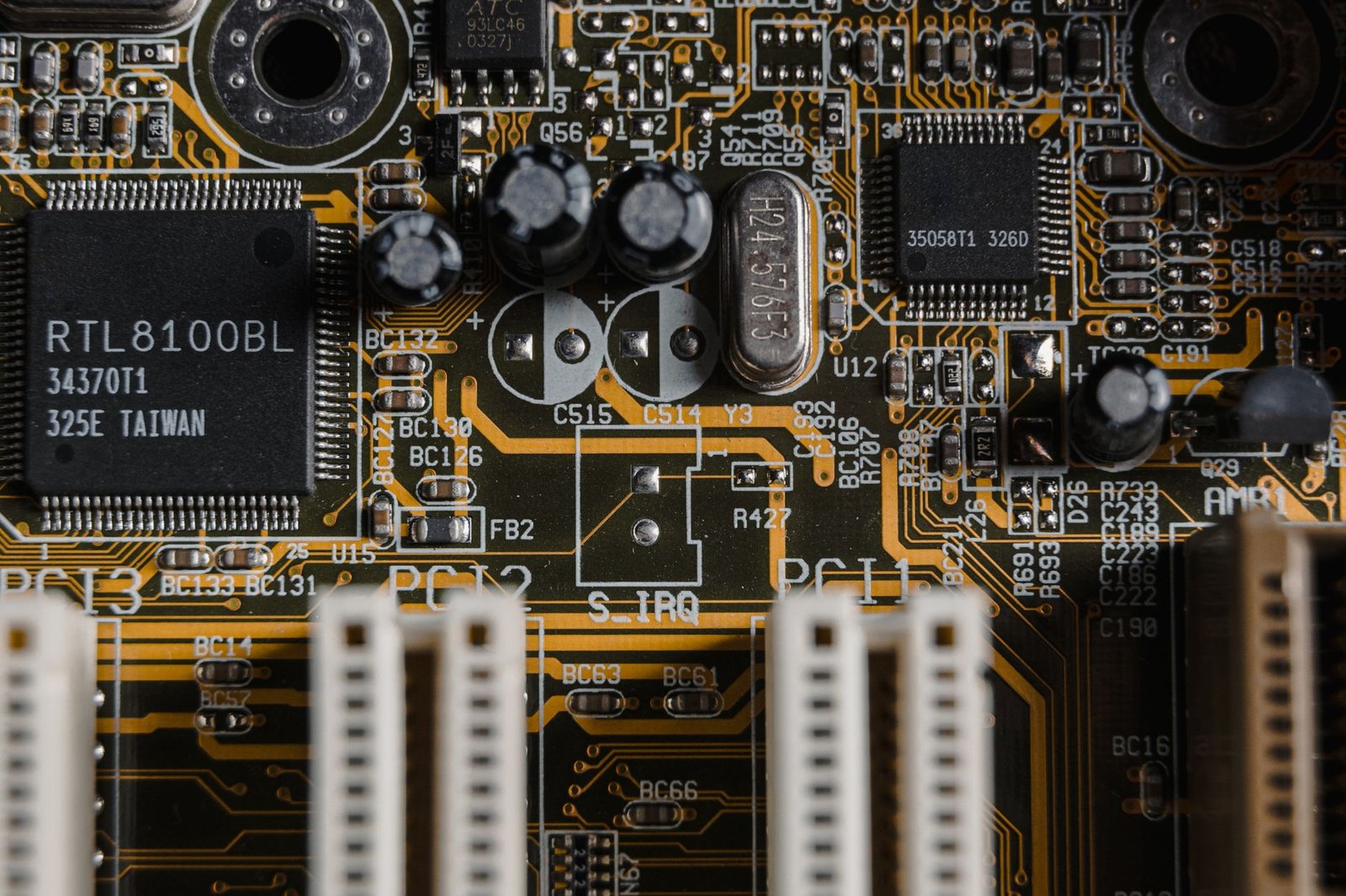
The semiconductor industry is undergoing a tectonic shift. Not on the process node front—where Intel, TSMC, and Samsung still fight over nanometers—but in advanced semiconductor packaging, the overlooked back-end technology that stitches chiplets together. Intel’s just-announced collaboration with Lens Technology, a Chinese specialist in precision glass manufacturing, could be the move that reshapes AI hardware economics. It’s a bet on glass substrates as the next interconnection medium—and a direct challenge to TSMC’s dominance with its CoWoS (Chip-on-Wafer-on-Substrate) packaging empire.
The partnership, articulated through an Intel Newsroom release, brings together Intel’s chip design and foundry muscle with Lens’s expertise in ultra-thin, ultra-flat glass processing. The goal: develop next-generation packaging substrates that can handle the immense bandwidth, power, and thermal demands of tomorrow’s AI accelerators. For enterprises evaluating GPU/accelerator roadmaps, this isn’t just an Intel lab experiment. It has the potential to crack open a bottleneck that’s been driving up AI chip costs and limiting supply.
Key Takeaways
- Intel is weaponizing glass substrates to leapfrog organic-package limitations, targeting AI workloads that demand extreme interconnect density and signal integrity.
- Lens Technology brings scalable, high-yield glass manufacturing, potentially lowering the cost of advanced packaging—a sore point for cloud providers and AI startups reliant on TSMC’s expensive CoWoS.
- This collaboration validates Intel’s foundry-first turnaround, offering chip designers a credible alternative to the TSMC packaging ecosystem and reducing single-supplier risk for the AI supply chain.
- Geopolitical complexities remain high, as reliance on a Chinese partner for critical packaging materials adds supply-chain fragility that IT procurement teams must weigh.
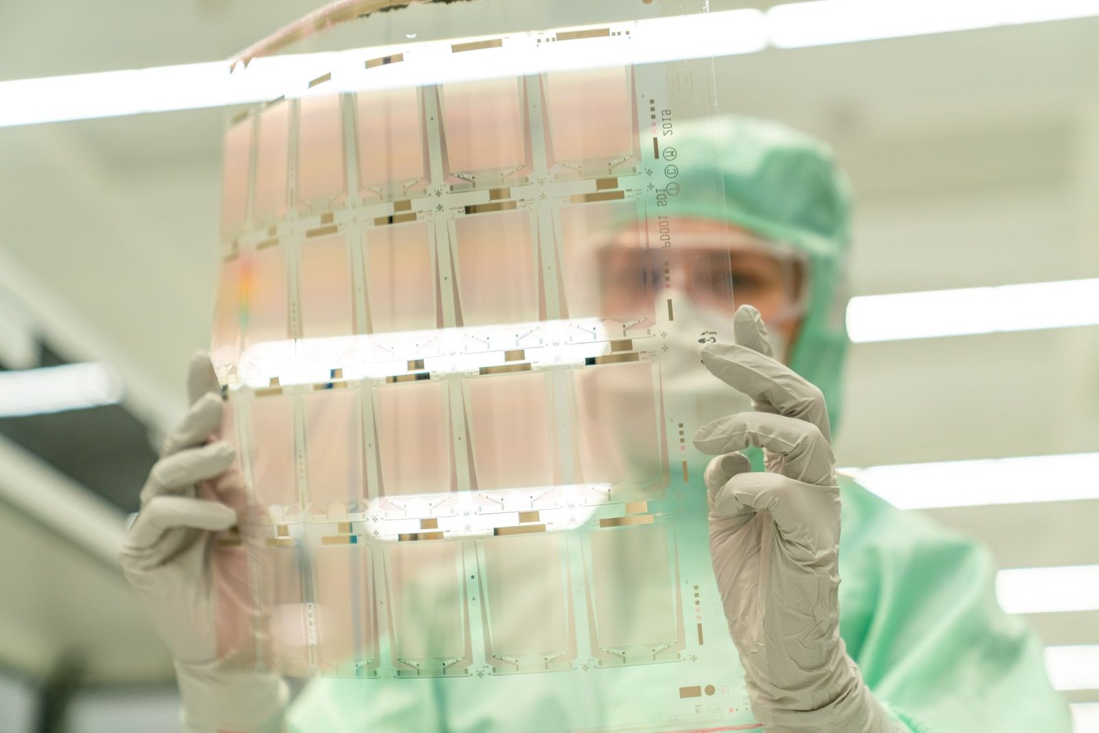
Deep Dive: Technology Review
At its core, advanced packaging is about connecting multiple chiplets—CPU cores, GPU tiles, I/O dies, HBM memory—onto a single substrate, so they behave like one monolithic chip. For AI workloads, where memory bandwidth and latency are everything, the substrate’s material properties directly affect performance. Until now, the industry has relied on organic resin-based substrates. These work, but they warp under heat, limit wiring density, and struggle with the power delivery requirements of 800-watt GPU monsters.
Intel’s bet, reinforced by the Lens partnership, is on glass. Glass substrates offer significantly flatter surfaces (enabling finer lithography for interconnects), lower dielectric loss for high-speed signals, and better thermal stability. Intel first teased its glass substrate roadmap in 2023, targeting volume production by the end of this decade. The collaboration with Lens accelerates that timeline by tapping Lens’s deep manufacturing know-how in ultra-thin glass—the same expertise that supplies smartphone giants with durable, precisely machined glass covers.
From a technical standpoint, the integration likely involves Intel’s existing EMIB (Embedded Multi-die Interconnect Bridge) and Foveros Direct 3D stacking but with a glass core replacing the organic substrate. This would allow up to 10x higher interconnect density than existing organic packages, per Intel’s prior research disclosures [SOURCE: Intel research paper on glass substrates, 2023]. The result: AI chips that can pack more chiplets into a single package, shuttle data faster, and dissipate heat more efficiently—key for training runs that can last weeks.
But there are trade-offs:
- Manufacturing maturity: Glass is brittle and challenging to process at the volumes and defect densities required. Lens’s expertise helps, but ramping to millions of units per year is unproven.
- Ecosystem lock-in: Intel’s packaging technology, however advanced, is tightly coupled to its own design tools and foundry processes. Chip designers evaluating Intel Foundry must weigh the benefits of glass substrates against the switching costs from TSMC’s mature ecosystem.
- Cost reality check: While glass promises lower material costs than complex organic interposers, the initial R&D and tooling will be expensive. The total cost of ownership for an AI chip using glass packaging may only undercut TSMC’s CoWoS-S/R variants after several years of production [SOURCE: semiconductor packaging cost analysis by Yole Group].
Industry Impact & Competitors
The advanced packaging market, currently dominated by TSMC, is projected to exceed $50 billion by 2028 as chiplet adoption becomes mainstream. Intel’s move is the most credible assault yet on TSMC’s near-monopoly for high-end AI packaging. Below, we compare the key players.
| Vendor | Key Packaging Technology | Substrate Material | Strengths | Weaknesses |
|---|---|---|---|---|
| TSMC | CoWoS (CoWoS-S, -R, -L) | Silicon interposer / organic | Proven at scale, tightly integrated with Nvidia/AMD GPUs, massive HBM capacity | Expensive, capacity-constrained, limited alternative for customers |
| Intel | EMIB + Foveros (with glass substrate) | Glass (with Lens partnership) | Higher interconnect density, lower power, cost-reduction potential, foundry optionality | Not yet in volume production, ecosystem less mature, geopolitical risk around Chinese partner |
| Samsung | I-Cube, H-Cube | Organic / silicon | HBM integration for own AI accelerators, strong memory synergy | Smaller tool suite, limited third-party design wins outside Samsung Logic |
What’s missing from the table is the geopolitical dimension. Lens Technology is Chinese, and the U.S. government’s chip export controls are tightening. Even if the collaboration focuses on R&D and avoids direct technology transfer, any packaging supply chain that crosses U.S.-China lines will face scrutiny. For enterprises building AI infrastructure, that means Intel’s glass substrate solution may be more attractive for U.S.-aligned foundry strategies, but it’s not entirely decoupled from geopolitical risk.

Who Should (and Shouldn’t) Adopt This
The technology is not yet commercially available, but it’s a critical signal for technology planning horizons. Here’s how different enterprise personas should interpret the development:
- Cloud providers and hyperscalers: If you’re designing custom AI silicon (Google TPU, Amazon Trainium, Microsoft Maia), Intel’s glass packaging roadmap offers a long-awaited second source to TSMC. You can start design-technology co-optimization discussions now to gauge cost and performance trade-offs for your 2027–2028 accelerator refresh. Diversification is a strategic imperative.
- AI chip startups: For fabless companies that can’t get guaranteed CoWoS capacity from TSMC, Intel Foundry’s glass substrate promise is a competitive lifeline. However, you’ll need to adopt Intel’s design methodology and EDA flow. The earlier you engage, the better your shot at securing allocation and influencing the packaging roadmap.
- Enterprise IT buyers (end users): This is a “watch closely” signal. In the near term, it won’t change your hardware purchase decisions, but if it successfully commercializes by 2027, it could break the Nvidia-GPU pricing treadmill by enabling cheaper, more diverse AI accelerators. Factor this into your 3-year infrastructure roadmap.
- Defense and government contractors: Given Lens’s Chinese origin, proceed with extreme caution. Unless Intel can demonstrate a fully onshore glass supply chain, you should treat this packaging path as second-tier for classified workloads.
Frequently Asked Questions
What is advanced semiconductor packaging, and why does it matter for AI?
Advanced semiconductor packaging is the technology that connects multiple chiplets—compute tiles, memory, I/O—into a single package that functions like one big chip. For AI, it determines how fast data can move between logic and high-bandwidth memory, directly affecting training and inference performance, power consumption, and heat dissipation. Better packaging can deliver more AI compute per watt and per dollar, making it a crucial technical lever for next-generation accelerators.
How does Intel’s collaboration with Lens Technology benefit AI chip development?
Lens Technology brings deep expertise in manufacturing ultra-thin, perfectly flat glass at high volumes. By moving from organic substrates to glass, Intel aims to support 10x more interconnect density within a package, enabling larger, more powerful chiplets for AI workloads. This can lower latency, improve signal integrity, and ultimately reduce the cost per packaged chip—potentially making advanced AI hardware more accessible to a broader set of cloud providers and enterprises.
Is Intel challenging TSMC’s dominance in chip packaging with this move?
Yes, directly. TSMC’s CoWoS packaging is the current gold standard and is heavily used by Nvidia, AMD, and others for AI accelerators. Intel’s glass substrate technology, if it reaches volume production on schedule, would offer a viable alternative with potentially better performance and lower cost. It’s a cornerstone of Intel’s ambition to become a major foundry player, giving chip designers a credible second source and breaking the current capacity bottleneck that has kept AI chip prices high.
The Bottom Line
Intel’s collaboration with Lens Technology is not just another press release—it’s a strategic countermove in the AI hardware arms race. By betting on glass substrates, Intel is positioning itself to solve two of the industry’s biggest pain points: the soaring cost of advanced packaging and the over-concentration of supply at TSMC. For enterprise technology leaders, the message is clear: start pressure-testing your AI chip supply chain assumptions now, because the packaging landscape could look very different by the time your next major infrastructure refresh rolls around.